
“I DO not depend on figures at all,” said Thomas Edison. “I try an experiment and reason out the result, somehow, by methods which I could not explain.” And so it was that by testing 1,600 different materials, from coconut fibre to fishing line and even a hair from a colleague’s beard
, Edison finally found a particular type of bamboo which could be used, in carbonised form, as the filament in the first proper incandescent light bulb. He demonstrated it on New Year’s Eve 1879 at his laboratory in Menlo Park, New Jersey.
Materials science is rapidly transforming the way that everything from cars to light bulbs is made, Paul Markillie
The details of all this painstaking trial and error filled more than 40,000 pages of Edison’s notebooks, but his solution was soon superseded. By the start of the 20th century filaments were being made from tungsten, which burned brighter and lasted longer. For over 100 years the world was illuminated by light bulbs with tungsten filaments, and the light bulb became the cartoonist’s fixed shorthand for innovation of all sorts.
Now light bulbs are being replaced by light-emitting diodes (LEDs), which are more efficient at turning electricity into light than filaments are, and far longer-lived. LEDs first appeared in the 1960s as indicator lights on electrical equipment. Today they provide powerful illumination for buildings, streets and cars. In poor parts of the world they are bringing light to people who have never seen an old-fashioned bulb.
Both Edison’s light bulb and the LED are inventions of materials science, the process of turning matter into new and useful forms. But in the years between them both the materials and the science became much more complex. The semiconducting materials, such as germanium or silicon, from which LEDs are made, often with the careful addition of atoms of some other substance, require a different approach from that at Menlo Park. The sort of light they produce is fine-tuned by microscopic structures and the details of those extra atoms. Pace Edison, this sort of thing depends on a lot of figures—not to mention quantum theory.
The ability to understand the properties of materials at the tiniest scales not only lets people do old things better; it lets them do new things. In Edison’s day, using light to send messages was the province of the Aldis lamps that flashed messages in morse code from ship to ship. Laser diodes—semiconductor devices engineered to produce a much purer light than LEDs—can flicker on and off in a controlled way billions of times a second. In an astounding number of applications where information has to get from A to B—be those end points a DVD and a speaker, a bar code and a supermarket checkout or the two ends of a transatlantic fibre-optic cable—laser diodes are doing the work. For all its seeming abstraction, the virtual world is built on very real, very well-understood materials.
This is what some scientists describe as a “golden age” for materials. New, high-performing substances such as exotic alloys and superstrong composites are emerging; “smart” materials can remember their shape, repair themselves or assemble themselves into components. Little structures that change the way something responds to light or sound can be used to turn a material into a “metamaterial” with very different properties. Advocates of nanotechnology talk of building things atom by atom. The result is a flood of new substances and new ideas for ways of using them to make old things better—and new things which have never been made before.
University materials departments are flourishing, spawning a vibrant entrepreneurial culture and producing a spate of innovations (see box below). Many of these discoveries will fail to scale up from laboratory demonstration to commercial proposition. But some just might change the world, as light bulbs did.
Faster, higher, stronger
The understanding of the material world provided by a century of physics and chemistry accounts for much of the ever-accelerating progress. But this is not a simple triumph of theory. Instruments matter too. Machines such as electron microscopes, atomic-force microscopes and X-ray synchrotrons allow scientists to measure and probe materials in much greater detail than has ever been possible before.
A project at the International Centre for Advanced Materials at the University of Manchester shows such advances in action. In one of its labs scientists are using secondary ion mass spectrometry (SIMS) to study the way that hydrogen atoms—the smallest atoms there are—diffuse into materials such as steel, a process that can cause tiny cracks. SIMS works by bombarding a sample with a beam of charged particles, which causes secondary particles to be ejected from the surface. These are measured by an array of detectors to create an image with a resolution down to 50 nanometres (billionths of a metre). It does not just reveal the crystalline structure of the metal—and any flaws in it—but also determines chemical impurities, such as the presence of hydrogen. “We can now do in an afternoon what we once did in months,” says Paul O’Brien, a professor at the university. The hope is that BP, the oil company which is sponsoring the centre, will get better steels for its offshore and processing work as a result.
As well as having ever better instruments, the researchers are also benefiting from a massive increase in available computing power. This allows them to explore in detail the properties of virtual materials before deciding whether to try and make something out of them.
“We are coming out of an age where we were blind,” says Gerbrand Ceder, a battery expert at the University of California, Berkeley. Together with Kristin Persson, of the Lawrence Berkeley National Laboratory, Mr Ceder founded the Materials Project, an open-access venture using a cluster of supercomputers to compile the properties of all known and predicted compounds. The idea is that, instead of setting out to find a substance with the desired properties for a particular job, researchers will soon be able to define the properties they require and their computers will provide them with a list of suitable candidates.
Their starting point is that all materials are made of atoms. How each atom behaves depends on which chemical element it belongs to. The elements all have distinct chemical properties that depend on the structure of the clouds of electrons that make up the outer layers of their atoms. Sometimes an atom will pair off one of its electron with an electron from a neighbouring atom to form a “chemical bond”. These are the kind of connections that give structure to molecules and to some sorts of crystalline material, such as semiconductors. Other sorts of atom like to share their electrons more widely. In a metal the atoms share lots of electrons; there are no bonds (which makes metals malleable) and electric currents can run free.
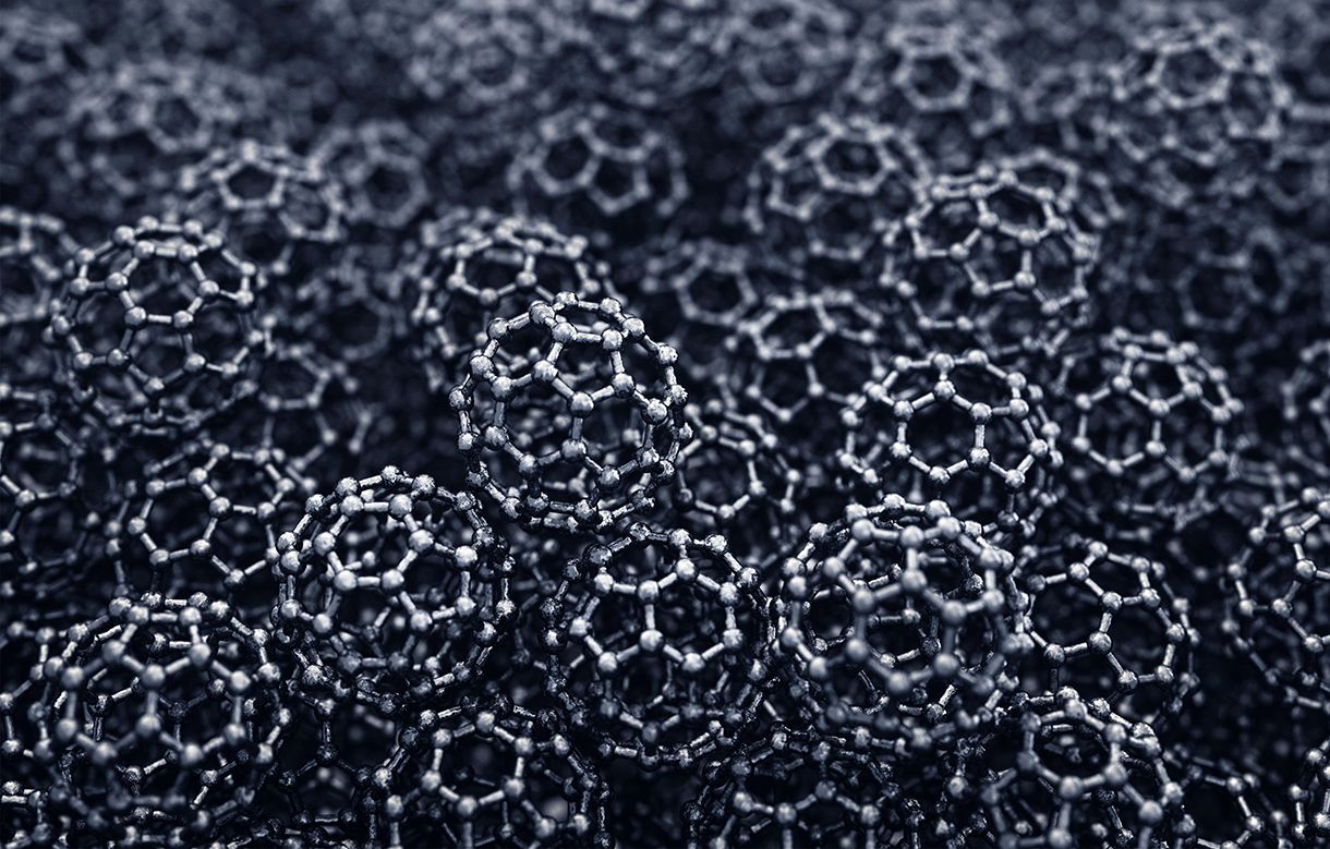
When it comes to making chemical bonds, one element, carbon, is in a league of its own; a more or less infinite number of distinct molecules can be made from it. Chemists call these carbon-based molecules organic, and have devoted a whole branch of their subject—inorganic chemistry—to ignoring them. Mr Ceder’s Materials Project sits in that inorganic domain. It has simulated some 60,000 materials, and five years from now should reach 100,000. This will provide what the people working on the project call the “materials genome”: a list of the basic properties—conductivity, hardness, elasticity, ability to absorb other chemicals and so on—of all the compounds anyone might think of. “In ten years someone doing materials design will have all these numbers available to them, and information about how materials will interact,” says Mr Ceder. “Before, none of this really existed. It was all trial and error.”